Here is one of the interesting 555 timer circuits to trick your friends while studying electronics in schools. Clap switch circuit is the local name of sound controlled flip flops. This sound controlled light can also be used as sound detection sensors. Flip flops are single bit storage elements. NE555 timer IC is the important part of this circuit. Here NE555 is configured in monostable multivibrator mode and is connected to the clock input of a 7474 D flip flop. The flip flop is connected to work in 'Toggle' mode. The relay circuit is energized by a 7474 flip flop. You can connect any electrical/electronic device at the output instead of the electrical bulb used here. Below is the electronic circuit diagram and working of the clap light switch.
Electronic circuit diagram of Clap switch
Click on the image to Enlarge
Components Required
- Bridge Rectifier (Step down Transformer, Diodes-4, and Capacitor 470μF)
- Condenser Mic
- Resistors (10KΩ, 1MΩ, 2.2KΩ, 220KΩ, 100Ω)
- Capacitors (0.1μF, 1μF)
- Transistors (BC 548, BC 187)
- NE 555 IC 7474
- 6V or 12V Relay (According to Vcc)
Working of Clap Switch Circuit
- Here the 555 IC operates in monostable multivibrator mode. It can be triggered with a low voltage at the 2nd pin.
- The collector voltage of BC 548 is connected to the trigger pin of 555.
- High amplitude sound signal in front of the condenser mic, turns ON the transistor BC 548.
- Then its collector voltage falls to low, and the 555 turns ON for a time 1.1RC sec.
- Output of the 555 is connected to clock input of D-flip flop (IC 7474). It is a -ve edge triggered flip flop. When the Monostable output goes to zero, flop-flop's output Toggles.
- Its output will be the input only after a clock pulse. Without the clock, output will be the same i.e. it will not affects the inputs.
- When Q' is connected to the D input, (say Q'=1) for the 1st clock pulse, Q=1 & Q'=0, for the next clock pulse Q=0 & Q'=1.
- That is (For time being consider flip-flop out is zero), for the 1st -ve transition output of the flip-flop goes to high and for the next -ve edge, output will be low. It will continue for successive -ve edges
- In this way we can hold the output as low or high.
- The flip flop out is connected to a relay, when the output of flip flop is high it will energize the relay coil.
- So the bulb connected on the relay will light up/down with each clap or any sound.
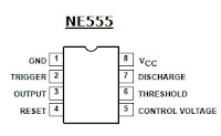
Components Pinout
Ads


+Circuit+diagram+using+CD4047+and+IRFZ44+power+MOSFET.png)


How to identify the terminals of Condenser mic
ReplyDeleteObserve the back side, one of the terminals have a connection to the body of condenser mic, that terminal is the ground.
Deletea new elekctronic swich a exampal 30km back a any elektical istument the start your poket data simply......a my new project
ReplyDeletei am not iti diploma cirtifect......
ReplyDeleteHello Govind, Welcome to i-St@r Technologies Lmtd. I didn't get you please explain detail. i-St@r group can support you in every electronic aspects.
Deletei make this circuit but it does n't work transistor bc548 is getting very hot after few sec so can u plz help me to recognize the problem in my circuit
ReplyDeleteHi akshay jha,
DeleteCheck if the pins of BC548 connected is correct, refer the pin diagram of BC548. Also check the transistor is damaged or not, connection error may damage transistor.
thank you for the circuit diagram , but i can't get the output .so would you give me the video of circuit connection for me
ReplyDeleteHi KAT Tie,
DeleteNice to see ya here. The circuit has been tested and verified under our i-St@r lab. Soon I'll upload the working video in this article.
How soon ? :(
DeleteHey Harsh,
DeleteI am looking forward to that, been busy last two days. You guys can expect it within 2 days. Follow us on google plus and like our facebook page. Keep visiting :)
Video has been UPLOADED!
DeleteBridge Rectifier is the rectifier diode (connected in parallel with relay). Right?
ReplyDelete